
YM2149F pinout
YM2149F / AY-3-8910 .–__–. GND -|01 40|- VCC NC -|02 39|- TEST Analog channel B output -|03 38|- Analog channel C output Analog channel A output -|04 37|- DA0 NC -|05 36|- DA1 I/O B 7 -|06 35|- DA2 I/O B 6 -|07 34|- DA3 I/O B 5 -|08 33|- DA4 I/O B 4 -|09 32|- DA5 I/O B 3 -|10 31|- DA6 I/O B 2 -|11 30|- DA7 I/O B 1 -|12 29|- BC1 I/O B 0 -|13 28|- BC2 I/O A 7 -|14 27|- BDIR I/O A 6 -|15 26|- /SEL (YM), TEST2 (AY) I/O A 5 -|16 25|- A8 I/O A 4 -|17 24|- /A9 I/O A 3 -|18 23|- /RESET I/O A 2 -|19 22|- CLK I/O A 1 -|20 21|- I/O A 0 ‘——’
- VCC, GND : power supply
- Audio channel outputs : analog outputs for 3 individual channels
- DA0-DA7 : data bus, can be either input, output or high-impedance
- A8, /A9 : upper address bits (the YM2149F can ignore data writes (even when the control mode was set to write mode) when address latch was written with DA4-DA7 nonzero or A8 and /A9 weren’t respectfully high and low)
- BDIR, BC1, BC2 : CP16xx-style data bus control (see below)
- I/O A, I/O B 0-7 : general-purpose I/O pins
- CLK : TTL-level clock input
- /SEL : enable internal ÷2 clock divider when this pin is low, not available in AY-3-8910
- /RESET : reset all 16 chip registers to “0” when this pin is pulled to low
- TEST, TEST2 : pins for factory testing, should be left floating
| BDIR | BC2 | BC1 | Action |
|---|---|---|---|
| 0 | 0 | 0 | No action |
| 0 | 0 | 1 | Address |
| 0 | 1 | 0 | No action |
| 0 | 1 | 1 | Read |
| 1 | 0 | 0 | Address |
| 1 | 0 | 1 | No action |
| 1 | 1 | 0 | Write |
| 1 | 1 | 1 | Address |
The data pins function as input in Write, Address mode, output in Read mode and go high-impedance in No action state.
Wiring with Sunsoft FME-7
For 6502-styled bus, the control pins can be treated like:
                I/O B 1 -|12  29|- GND
                I/O B 0 -|13  28|- A0
                I/O A 7 -|14  27|- +CS
                I/O A 6 -|15  26|- /SEL (YM), TEST2 (AY)
                I/O A 5 -|16  25|- VCC
                I/O A 4 -|17  24|- GND
Where A0 selects address latch when the pin is low, data write when the pin is high (this diagram does not consider Read mode).
The wiring for AY-3-8910 or YM2149F looks like this:
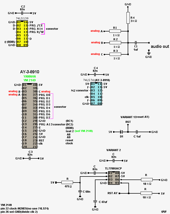
74'27 can be used instead for 74'139:
                          74LS27
                         .--__--.
                        -|01  14|-----------<[VCC]
                        -|02  13|-
        [CPU A14]>-+-----|03  12|-
                   +-----|04  11|-----------<[R/W]
                   +-----|05  10|-----------<[/ROMSEL]
                      +--|06  09|-------+
        [GND]>--------|--|07  08|--+    |
                      |  '------'  +--------<[YM BDIR]
                      |                 |
                      +-----------------+
                          74'138
                         .--__--.
                +--------|01  16|-----------<[VCC]
        [GND]>--+--------|02  15|-----------<[YM BDIR]
                +--------|03  14|-
        [/ROMSEL]>-------|04  13|-
        [R/W]>-----------|05  12|-
        [CPU A14]>-------|06  11|-
                        -|07  10|-
        [GND]>-----------|08  09|-
                         '------'
                          74'157
                         .--__--.
        [R/W]>-----------|01  16|-----------<[VCC]
                        -|02  15|-----------<[/ROMSEL]
                        -|03  14|-
                        -|04  13|-
    [CPU A14]>-----------|05  12|-
        [GND]>-----------|06  11|-
    [YM BDIR]>-----------|07  10|-
        [GND]>-----------|08  09|-
                         '------'